WAVELIGHT TECHNOLOGIES
APPLICATION
Spectroscopy & Diagnostics
-
Laser-induced plasma has become a cornerstone technology across various diagnostic and industrial applications, including material detection, thin-film deposition, and elemental identification. Laser-Induced Plasma Spectroscopy (LIPS)—also known as LIBS or Laser Spark Spectroscopy (LSS)—offers a powerful platform for rapid, in-situ analysis of solid, liquid, and gaseous samples.
This technique is widely used in:
Real-time monitoring in the steel industry
Material inspection and leakage detection in power plants
Environmental analysis of soils and water
Cultural heritage object examination
Explosive identification and security applications
Planetary exploration and surface characterization
Pulsed Laser Deposition (PLD)
Pulsed Laser Deposition is among the most straightforward and versatile physical vapor deposition (PVD) techniques. A high-power pulsed laser is focused inside a vacuum chamber to ablate a target material, allowing precise control of film composition and structure. Conceptually simple yet highly effective, PLD remains one of the most practical and clean thin-film growth methods.
Advanced Applications of Laser-Produced Plasma (LPP)
With the rapid development of short-pulse laser systems, new plasma-based technologies continue to emerge. Extreme Ultraviolet (EUV) sources based on laser-produced plasmas, emitting at wavelengths in the tens of nanometers, are being actively developed for next-generation semiconductor lithography.
These sources are crucial for:
High-volume manufacturing of semiconductor devices
Mask inspection and actinic metrology
Optics and sensor testing
Material characterization at nanometer scales
Compact LPP sources are also used to generate soft X-ray (SXR) radiation, enabling laboratory-scale systems for:
High-resolution microscopy
Absorption spectroscopy in the water-window range (2.2–4.4 nm)
Ultrafast X-Ray Diagnostics
The availability of synchrotron and laser-plasma X-ray sources has significantly advanced time-resolved X-ray diagnostic techniques, including:
Time-resolved X-ray diffraction (TR-XRD)
Streak-camera X-ray detection
CCD-based X-ray imaging technologies
Specialized scintillation detection systems
These innovations have fundamentally expanded the capabilities of ultrafast material studies, enabling deeper insights into structural dynamics, high-energy-density physics, and advanced photonic applications.
-
Photodissociation—also known as photolysis or photodecomposition—is a fundamental photochemical process in which a chemical compound is broken down by photons. It occurs when one or more photons interact with a target molecule, leading to bond cleavage and the formation of new chemical species.
Photolysis plays a crucial role in natural processes such as photosynthesis, where the absorption of light by chlorophyll drives the splitting of water molecules into oxygen gas and hydrogen ions. This reaction takes place in the grana of chloroplasts and provides the energy required for further biochemical transformations.
Laser Flash Photolysis (LFP)
Laser Flash Photolysis is an advanced technique used to study transient chemical and biological species generated by short, intense light pulses from nanosecond, picosecond, or femtosecond pulsed laser sources. A high-energy pump pulse excites the sample and produces short-lived intermediates—such as excited states, radicals, and ions—in sufficiently high concentrations to allow detailed observation.These intermediates are monitored via time-resolved absorption measurements using probe pulses, enabling precise analysis of relaxation dynamics and reaction pathways. The integration of Optical Parametric Oscillators (OPOs) expands spectral coverage, making LFP a powerful tool for molecular spectroscopy, reaction kinetics, and photochemical research.
-
Sum Frequency Generation Vibrational Spectroscopy (SFG-VS) is a powerful and highly selective technique for probing the vibrational structure of molecules at surfaces and interfaces. Unlike conventional spectroscopic methods that capture bulk responses, SFG spectroscopy delivers intrinsic interfacial sensitivity and molecular-level specificity.
This surface sensitivity arises from the fact that nonlinear sum-frequency generation is forbidden in centrosymmetric media but becomes allowed at interfaces where inversion symmetry is broken. In an SFG measurement, a tunable infrared beam resonant with molecular vibrations is combined with a visible beam to generate light at the sum frequency, which can be detected efficiently in the visible range.
-
Second Harmonic Generation (SHG) is a second-order nonlinear optical process in which two photons of frequency ω combine to produce a single photon at 2ω. This process occurs exclusively in non-centrosymmetric media, providing exceptional surface and structural sensitivity.
SHG spectroscopy enables detailed analysis of molecular orientation, adsorption dynamics, and interfacial chemical reactions. SHG microscopy extends these capabilities into high-resolution imaging, offering label-free visualization of ordered biological and crystalline structures such as collagen fibers, myosin filaments, and ferroelectric domains.
-
Pump-probe spectroscopy enables direct observation of ultrafast chemical, physical, and biological processes by using two precisely timed laser pulses. The pump pulse excites the system, while the delayed probe pulse monitors its response.
By scanning the delay between pulses, researchers construct a time-resolved picture of excited-state relaxation, energy transfer, photochemical reactions, plasma formation, and structural dynamics across timescales from femtoseconds to nanoseconds.
-
Time-Resolved Photoluminescence (TRPL) Spectroscopy is a non-contact, high-precision technique for probing recombination processes and charge carrier dynamics in solid materials. By exciting luminescence from a sample using a pulsed light source and measuring the decay of emitted light over time, TRPL provides critical insights into the intrinsic properties of semiconductors, nanostructures, and optoelectronic materials.
How TRPL Works
In TRPL experiments, a pulsed laser excites the sample, generating luminescence that is subsequently monitored using sensitive detectors such as photodiodes, photomultiplier tubes (PMTs), or streak cameras configured for upconversion or single-photon counting. The temporal resolution, wavelength range, and detection sensitivity can be optimized for each application, allowing precise characterization of material dynamics.
Applications and Advantages
TRPL is particularly valuable for lifetime imaging of charge carriers, providing insight into nonradiative surface recombination at semiconductor boundaries. Understanding and controlling these recombination processes is essential for improving the efficiency of:
Light-emitting diodes (LEDs) and laser diodes (LDs)
Photovoltaic cells
Photodetectors
The effective carrier lifetime measured through TRPL is a key parameter for optimizing solar cell conversion efficiency and overall device performance.
Photoluminescence Microscopy
Beyond spectroscopy, photoluminescence microscopy allows high-resolution imaging of crystal defects and structural inhomogeneities in semiconductors and organometallic complexes. This makes it an essential tool for:
Nanostructure fabrication and characterization
Manufacturing of high-performance optoelectronic devices
Quality control in solar cell and photodetector production
With its contactless, non-destructive, and highly sensitive approach, TRPL combined with photoluminescence microscopy provides unparalleled insight into material behavior, enabling innovation in both research and industrial applications.
-
Gas-phase ion luminescence spectroscopy is a powerful technique for probing the intrinsic electronic transition energies of ions in the absence of environmental perturbations. By isolating ions in the gas phase, this method allows researchers to study molecular properties with unparalleled precision and clarity.
How It Works
Large ions generated via electrospray ionization (ESI) are stored and mass-selected within a cylindrical Paul trap. These trapped ions are then irradiated using a tunable 20-Hz pulsed laser from EKSPLA, and the resulting emitted photons are detected. The low repetition rate of the laser ensures that mass selection occurs between each irradiation event, eliminating fluorescence contributions from ion impurities and enabling clean, high-resolution spectra.
The tunable nature of the laser allows excitation of a wide range of dye molecules, producing luminescence across various wavelengths. For example, oxazine dye cations display emission spectra spanning 500–750 nm, illustrating the versatility of the technique in studying different molecular systems.
Applications in Biomolecular Structure
Gas-phase ion luminescence spectroscopy is not limited to dyes—it is also a powerful tool for investigating three-dimensional structures of peptides and nucleic acids using Förster Resonance Energy Transfer (FRET). Biomolecules are labeled with donor-acceptor dye pairs, such as Rhodamine 575 and 640. Structural information is derived from the efficiency of energy transfer, which is highly sensitive to the distance between donor and acceptor dyes (inversely proportional to the sixth power of the distance), allowing precise mapping of molecular conformations in the gas phase.
Why It Matters
This technique provides direct, high-resolution insight into molecular electronic states and structural configurations, making it invaluable for:
Fundamental photophysical studies of ions
Spectroscopic characterization of complex biomolecules
Investigation of energy transfer processes and molecular interactions
Advanced research in chemistry, biophysics, and material sciences
By combining mass selection, tunable excitation, and photon detection, gas-phase ion luminescence spectroscopy offers an unmatched platform for detailed, impurity-free spectroscopic analysis of ions and biomolecules.
-
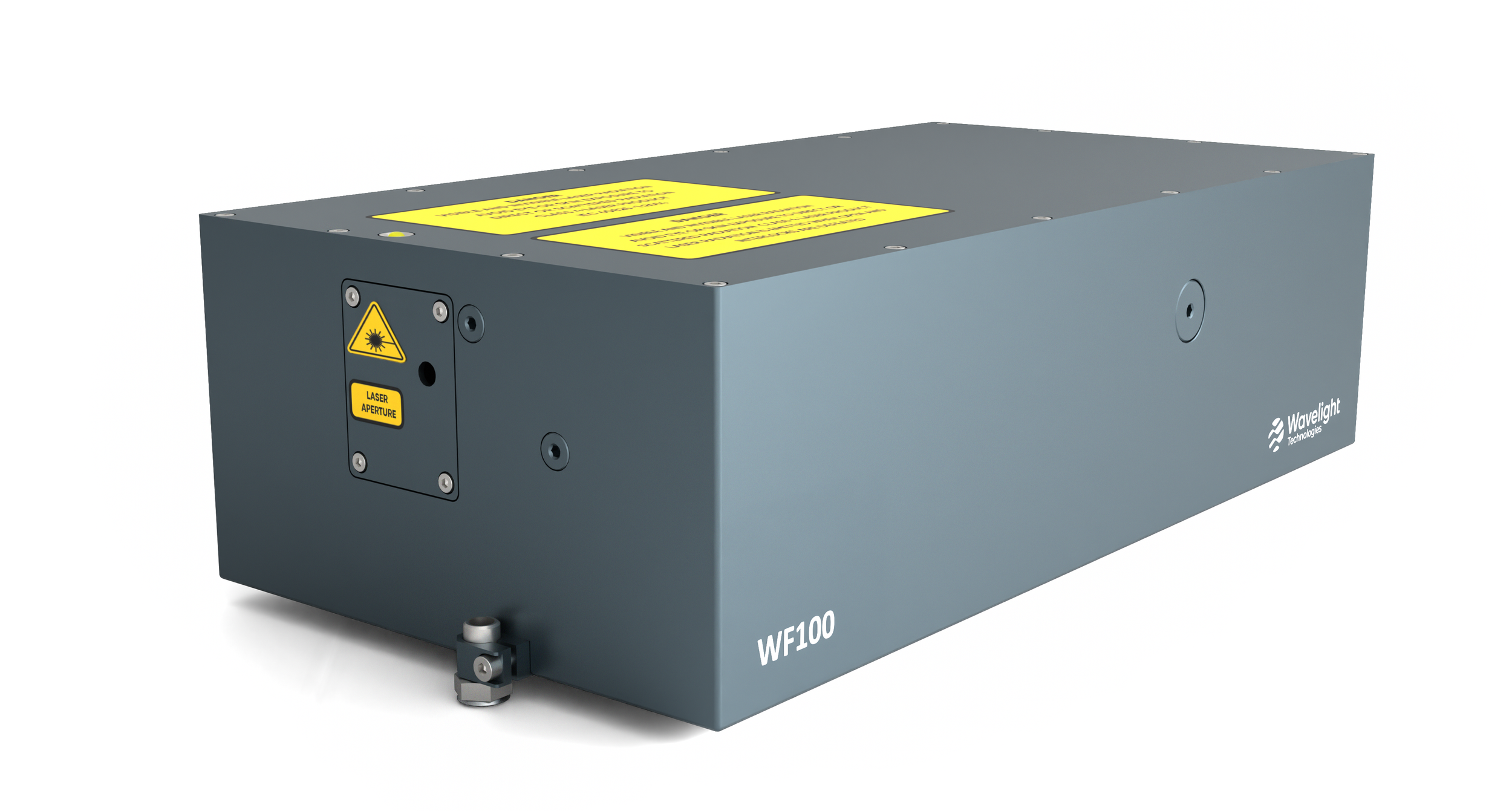
Supercontinuum lasers, often referred to as “white light lasers,” have emerged as a turn-key fiber-laser technology widely used across fields ranging from biomedical imaging to optical device characterization. Their popularity stems from a unique combination of broad spectral coverage, high output power, and diffraction-limited beam quality, making them a versatile and powerful light source for research and industrial applications.
Key Features
Extremely broad spectral range: 400 nm – 2400 nm
High optical output power: several watts
Diffraction-limited Gaussian beam: for precise focusing and imaging
Turn-key operation: fully integrated fiber-based systems for ease of use
How It Works
Most commercial supercontinuum sources are fully fiber-based, consisting of:
A mode-locked fiber oscillator serving as the master seed laser, typically producing picosecond pulses around 1064 nm with repetition rates in the tens of MHz.
A fiber amplifier to boost the pulse peak power.
A few meters of photonic crystal fiber (PCF) with engineered dispersion, where nonlinear interactions generate the broadband supercontinuum output.
When combined with a tunable spectral filter, the supercontinuum laser transforms into a widely tunable light source, enabling flexible and precise control over the output wavelength for a variety of scientific and industrial applications.
Applications
Supercontinuum lasers are highly versatile and are used in:
Biomedical imaging (e.g., optical coherence tomography, multiphoton microscopy)
Spectroscopy and optical characterization of materials and devices
Laser-based metrology and high-resolution imaging
Nonlinear optics and photonics research
With their unmatched spectral coverage, tunability, and high beam quality, supercontinuum sources provide a reliable and adaptable platform for both research and industrial applications requiring broadband, high-intensity light.
-
Time-Resolved Microwave Photoconductivity (TRMC) is a contactless, high-precision technique for characterizing charge carrier dynamics in a wide range of materials, including organic semiconductors, dyes, inorganic semiconductors, and metal-insulator composites. These materials are widely used in thin-film transistors, light-emitting diodes (LEDs), conductive inks, photocatalysts, and photovoltaic devices.
How TRMC Works
TRMC measures the photoconductivity response of a material following pulsed photoexcitation. By analyzing the time evolution, photon energy dependence, light intensity, temperature effects, and frequency response, researchers can gain detailed insight into:
Carrier generation and density
Charge transport and mobility
Trapping and recombination dynamics
These measurements allow precise evaluation of the material’s electronic properties without physical contacts, preserving sample integrity and enabling studies of delicate or complex materials.
Applications and Advantages
TRMC has become an essential diagnostic tool for next-generation electronic materials and devices. Its high sensitivity and temporal resolution provide valuable guidance for:
Optimizing charge transport in semiconductors
Evaluating photovoltaic efficiency
Improving performance of LEDs and thin-film devices
Investigating novel conductive and photoactive materials
With a robust theoretical framework supporting the interpretation of results, TRMC enables reliable, quantitative insights into fundamental carrier dynamics, making it a cornerstone technique in modern materials research and device development.
-
The Z-scan technique is a widely used method in nonlinear optics to measure the nonlinear refractive index (n₂, Kerr nonlinearity) and the nonlinear absorption coefficient (Δα). By employing closed- and open-aperture configurations, Z-scan allows the precise determination of both the real and imaginary components of a material’s nonlinear optical response.
Measuring Nonlinear Refraction (n₂)
To determine the real part of the nonlinear refractive index, the closed-aperture Z-scan configuration is employed. In this setup:
The sample is positioned near the focal plane of a lens.
The sample is moved along the z-axis (defined by the Rayleigh length).
The nonlinear material behaves like a weak z-dependent lens, causing subtle distortions in the transmitted beam.
By analyzing the far-field beam distortions captured by a detector and interpreting the data with theoretical models, the nonlinear refractive index (n₂) of the material can be accurately extracted.
Measuring Nonlinear Absorption (Δα)
The imaginary part of the nonlinear refractive index, or the nonlinear absorption coefficient, is measured using the open-aperture Z-scan. In this configuration:
The far-field aperture is removed, allowing the detector to capture the entire transmitted beam.
Beam distortions are negligible, so the z-dependent signal variation arises solely from nonlinear absorption effects.
The primary mechanism of nonlinear absorption is two-photon absorption (TPA), which becomes significant under high-intensity pulsed laser illumination.
Laser Requirements
Due to the need for high peak intensities and practical cost considerations, picosecond high-energy lasers are typically the preferred light source for Z-scan measurements. This makes the technique ideal for investigating a wide range of nonlinear optical materials efficiently and accurately.
Applications
Z-scan is a critical tool in:
Characterizing optical materials for photonics and laser applications
Measuring nonlinear coefficients for optical switching and modulation
Studying two-photon absorption in semiconductors, polymers, and nanomaterials
Guiding the design of nonlinear optical devices for telecommunications, imaging, and sensing
With its sensitivity, precision, and versatility, Z-scan remains a cornerstone method in nonlinear optics research and material characterization.
-
LIDAR, short for Light Detection and Ranging, is a powerful remote sensing technology that uses short laser pulses to measure distances and map objects with exceptional precision. By sending laser pulses into the atmosphere, LIDAR detects scattering from particles, aerosols, and air molecules, which is collected by a telescope and analyzed. Since the speed of light is constant, the time delay of the returning signal provides accurate spatial information along the beam path.
Key Features
Operates across ultraviolet, visible, and near-infrared wavelengths
Capable of imaging diverse materials, including non-metallic objects, rocks, rain, aerosols, clouds, pollutants, and even single molecules
Provides high-resolution distance measurements and three-dimensional mapping
Ideal for remote or hard-to-access environments where conventional methods are limited
Applications
LIDAR technology is widely used in:
Environmental monitoring: tracking aerosols, pollutants, and clouds
Geospatial mapping and surveying of terrain, vegetation, and structures
Industrial and scientific research requiring precise measurement of distances and spatial structures
Atmospheric studies to analyze chemical composition and particle distribution
With its precision, versatility, and ability to operate remotely, LIDAR has become an essential tool in environmental science, engineering, and advanced research applications.
Material Processing & Manufacturing
-
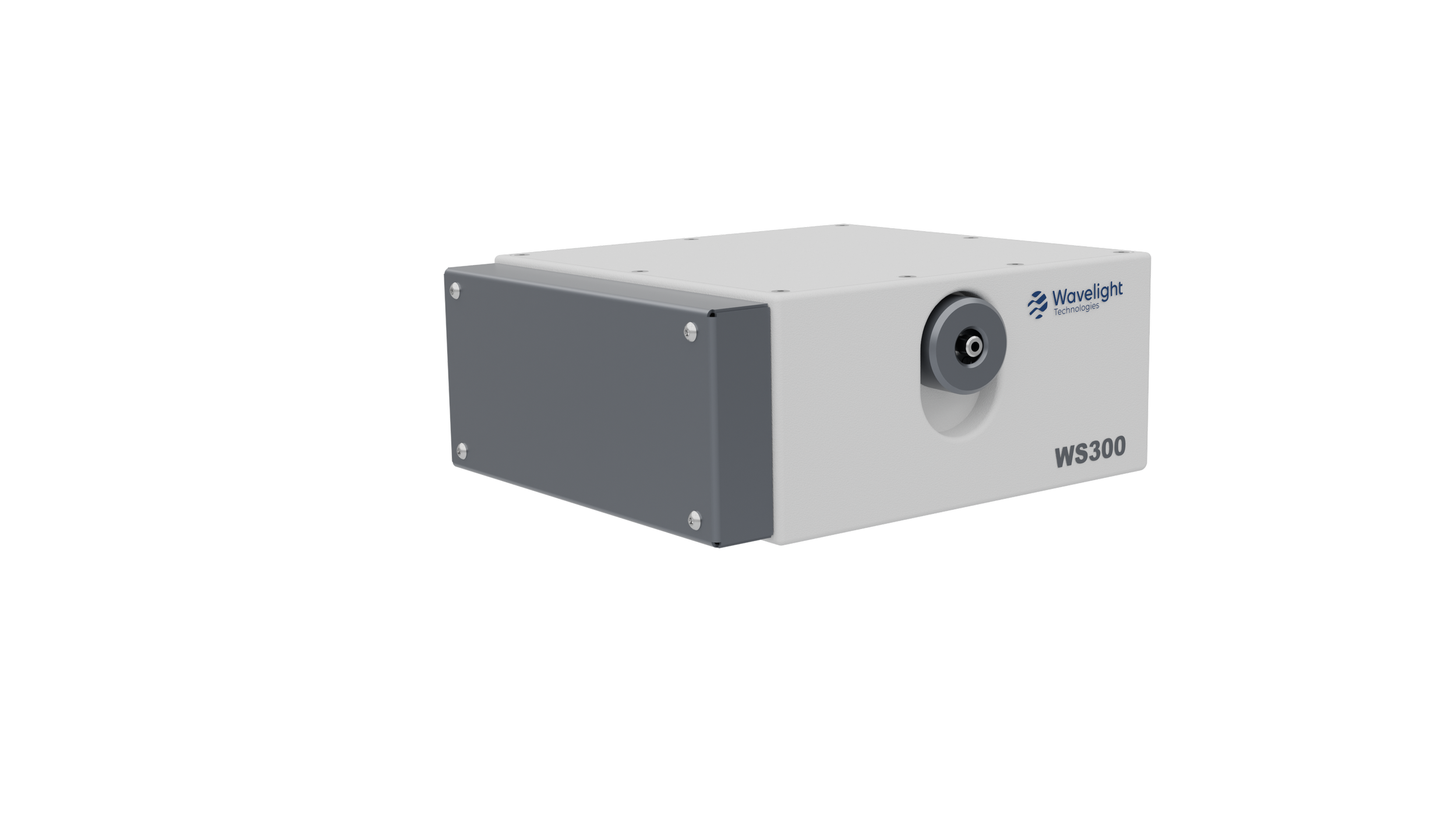
Photopolymerization is a cutting-edge microfabrication technique that enables the creation of highly complex three-dimensional polymer structures with micrometer-scale precision. By selectively solidifying photosensitive resins through spatially controlled laser-induced polymerization, it allows the fabrication of intricate 3D architectures with arbitrary shapes, sizes, and thicknesses. This versatility makes photopolymerization ideal for a wide range of applications, including tissue engineering, microelectronics, photonics, and microfluidic systems. The process provides true volumetric fabrication with sub-micrometer accuracy, minimal thermal impact on surrounding materials, and the ability to produce highly detailed structures that would be challenging or impossible with conventional fabrication methods. High-throughput approaches can further accelerate production, making photopolymerization a powerful tool for both research and industrial-scale microfabrication.
-
Femtosecond laser marking enables precise and permanent labeling of metals, plastics, and glass with unparalleled accuracy. This technology allows the creation of serial numbers, logos, barcodes, and traceable information for quality control, ensuring full product traceability and compliance in industrial and manufacturing processes. Beyond simple identification, laser-based marking can functionalize surfaces at the micro- and nanoscale, creating patterns that enhance light absorption, control wettability, improve tribological performance, and even provide antibacterial properties. These capabilities make laser marking an ideal solution for high-value components, master molds, medical devices, and electronics, delivering high-speed, durable, and contamination-free marking while enabling advanced automation and repeatability across production lines. By combining precision with functional versatility, femtosecond laser marking transforms ordinary surfaces into highly controlled, engineered materials ready for modern industrial and scientific applications.Education, R&D and Government Institutions
-
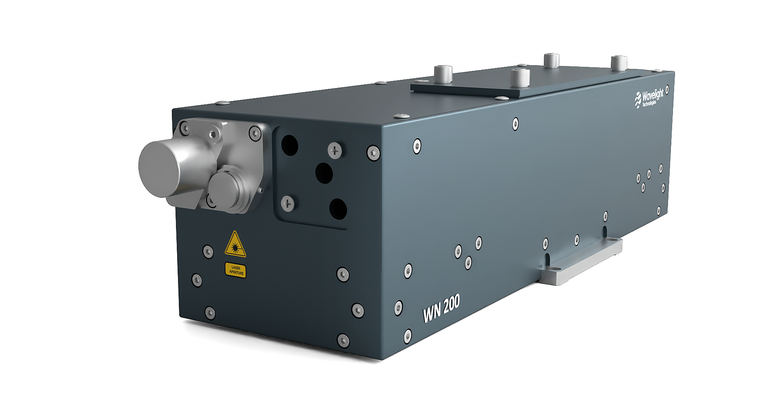
Ablation laser systems are advanced tools that enable precise material removal, modification, and structuring through the controlled application of laser energy. By rapidly heating, melting, and vaporizing or sublimating the target material, these systems allow non-contact, high-precision processing at micro- and nanoscale levels. The process can be finely controlled by adjusting parameters such as laser wavelength, pulse duration, energy density, and repetition rate, ensuring accurate and reproducible results across a wide range of materials. Ablation laser systems are employed in diverse applications, including cutting, drilling, and micromachining of metals, ceramics, polymers, and composites; medical procedures such as skin resurfacing, tattoo removal, and ophthalmic surgeries; electronics manufacturing for patterning, structuring, and MEMS fabrication; research and development for material analysis and thin-film preparation; and surface cleaning or restoration, including removing coatings, oxidation layers, or contaminants from delicate surfaces. With minimal thermal effects, high versatility, and exceptional precision, ablation laser systems provide an indispensable solution for industries and research fields that require detailed, reliable, and non-contact material processing.
-
Pulsed Laser Deposition (PLD) is a versatile technique for depositing thin films and multilayers on various substrates, including silicon wafers. In PLD, a high-power pulsed laser beam is focused onto a target material, generating a plasma plume that deposits the material onto a substrate. This process can occur in ultra-high vacuum or in the presence of a background gas, such as oxygen, which is commonly used for depositing oxides to ensure full oxygenation of the films.
Laser Options and Advantages
While Excimer lasers have traditionally been used for PLD due to their high-energy UV pulses, solid-state lasers (such as Nd:YAG) now offer significant advantages:
Higher energy density at the target: Nd:YAG lasers produce smaller, round, and more intense beams, delivering the required fluence with lower pulse energy compared to the larger, rectangular Excimer beams.
Flexibility in wavelength selection: Nd:YAG systems allow tuning across multiple wavelengths (e.g., 266 nm, 355 nm, 532 nm, 213 nm, 1064 nm) by adjusting optical components, enabling processing of a wide range of materials and substrates.
Lower cost of ownership: Solid-state lasers require minimal maintenance, with easily replaced components such as flashlamps and filters. In contrast, traditional gas-based Excimer lasers require periodic replacement of expensive gases and electrodes, adding complexity and cost.
Process Stability
Stable laser fluence is critical for consistent film quality, stoichiometry, and deposition rate. Modern solid-state lasers feature continuous auto-tuning, maintaining constant energy output over extended operation periods. This stability is particularly important when operating in the UV range, where harmonic crystals may self-heat, causing natural drift in pulse energy. Reliable output ensures uniform thin films and reproducible material properties across deposition runs.
Applications of PLD
PLD is widely used in the fabrication of:
Oxide thin films for electronics and photonics
Multilayer coatings with precise compositional control
Functional nanomaterials for optoelectronics, photovoltaics, and sensors
Research and development of advanced material systems
-
Nanomaterials, defined as materials with at least one dimension below 100 nm, exhibit unique physicochemical properties that differ significantly from their bulk counterparts. These size- and shape-dependent properties—including enhanced mechanical, optical, magnetic, and electronic characteristics—have revolutionized both the fabrication of nanomaterials and their applications across science and technology. By tailoring materials at the nanoscale, it is possible to achieve highly specific surface areas and optimized functional properties, opening new frontiers in research and industry.
Nanofabrication Approaches
Nanostructures can be produced using two main strategies:
Top-down methods: Reducing bulk materials to nanoscale dimensions through physical or chemical approaches such as electron/ion beam lithography, milling, laser ablation, and reactive ion etching.
Bottom-up methods: Assembling atoms or molecules to construct nanostructures via techniques like chemical and physical vapor deposition (CVD and PVD), epitaxial growth, and self-assembly.
Laser-Based Nanomaterial Synthesis
Among nanofabrication techniques, laser-based methods offer outstanding advantages, including high production efficiency, precise control over size and shape, low cost, environmental friendliness, and reliable quality. Common laser-based techniques include:
Laser Ablation and Vaporization – Efficiently produces nanoparticles and nanostructures in various atmospheres.
Pulsed Laser Deposition (PLD) – Creates high-quality thin films and nanostructured coatings.
Laser-Chemical Vapor Deposition (LCVD) – Enables controlled growth of nanostructures with specific properties.
Laser Synthesis and Processing of Colloids (LSPC) – Produces ligand-free nanoparticles in liquids, allowing high surface purity, alloy formation, or doped nanomaterials.
Three main LSPC approaches are used:
Laser Ablation in Liquids (LAL): A laser scans a bulk target in liquid to produce colloidal nanoparticles.
Laser Fragmentation in Liquids (LFL): Microparticle suspensions or colloids are irradiated to fracture particles.
Laser Melting in Liquids (LML): Primary nanoparticles are melted into larger, uniform particles.
Applications and Advanced Studies
Laser-based nanofabrication enables the creation of bimetallic, core–shell, and alloy nanoparticles with tailored properties. For example:
Au/Ag nanoparticles synthesized in supercritical CO₂ can form alloys or core–shell structures depending on laser configuration.
MoSx/WSe₂/C(B)/Al₂O₃ photocathodes produced via PLD show promise for solar water splitting, achieving a current density of ~3 mA/cm² at 0 V (RHE) and an onset potential of 400 mV (RHE).
Air-stable Cu nanoparticles synthesized by femtosecond laser irradiation of copper acetylacetone solutions demonstrate long-term stability and excellent photocatalytic performance.
Why Laser-Based Nanofabrication Matters
Laser-assisted synthesis provides unmatched precision, scalability, and versatility, enabling the production of nanomaterials with controlled size, shape, composition, and functionality. These capabilities drive innovation in optoelectronics, photovoltaics, catalysis, and advanced materials research, establishing laser-based nanofabrication as a cornerstone of modern nanotechnology.
-
Lasers play a critical role in the fabrication and quality control of electronic displays and semiconductor devices, enabling higher precision, larger panels, and improved production efficiency.
Display Panel Manufacturing and Repair
Defect detection and repair: Machine vision systems identify defects in newly manufactured LCD and LED panels. Pulsed lasers can selectively ablate or melt defective areas, preventing dead pixels or spots and improving panel yield.
Laser lift-off: Pulsed lasers are used to release chips from substrates, such as RFID chips, which helps reduce production costs and supports automated assembly processes.
Photovoltaic Panel Processing
Cleaning and structuring: Pulsed lasers remove excess silicon and create isolation channels between solar cells, enhancing efficiency and enabling large-scale production of photovoltaic panels.
Energy optimization: Improved solar panel manufacturing contributes to more homes generating and returning surplus energy to the grid, reducing reliance on traditional power sources and lowering pollution.
Printed Circuit Board (PCB) Fabrication
Precision drilling: Lasers are used to drill micro-holes in multi-layer circuit boards, allowing through-hole plating and interconnection between conductors.
Marking and identification: Lasers can mark identifiers, codes, or logos on a variety of materials used in chips, PCBs, and circuit assemblies with high precision and durability.
Benefits of Laser Integration
Non-contact, high-precision processing
Reduced material waste and improved yield
Scalable for both small and large production volumes
Versatile across multiple materials and manufacturing steps
-
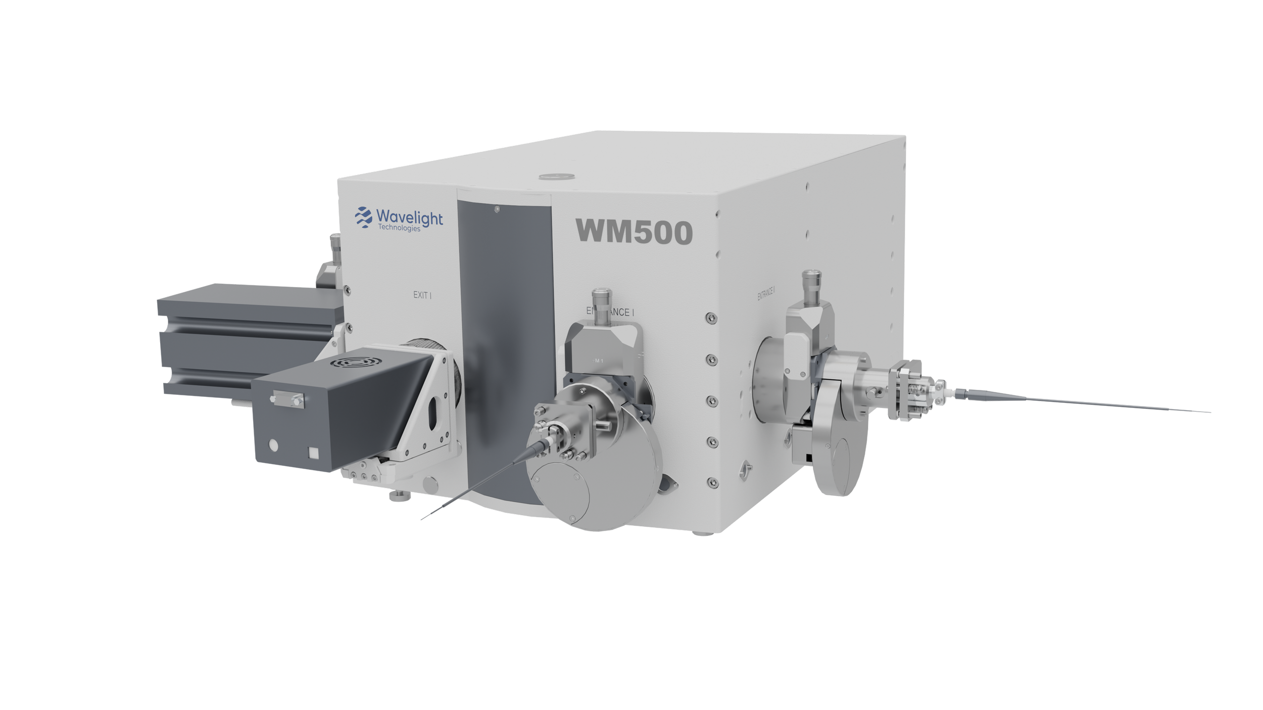
Advanced analytical techniques are essential for ensuring the quality, performance, and reliability of semiconductor materials. From detecting impurities and contaminants to analyzing defects and monitoring fabrication processes, these methods enable precise characterization of a wide range of semiconductors, including silicon, germanium, gallium arsenide, silicon carbide, and gallium nitride. By providing detailed insights into material composition, structural integrity, and particle size, semiconductor analysis supports process optimization, enhances device performance, and helps maintain the highest levels of productivity in electronics manufacturing and research. These capabilities are critical for developing next-generation semiconductor technologies and ensuring consistent, high-quality results across all stages of material processing and device fabrication.
-
MISSING CONTENT
FUNDAMENTAL RESEARCH & ADVANCED PHYSICS
-
Laser-induced plasma has become a cornerstone technology across various diagnostic and industrial applications, including material detection, thin-film deposition, and elemental identification. Laser-Induced Plasma Spectroscopy (LIPS)—also known as LIBS or Laser Spark Spectroscopy (LSS)—offers a powerful platform for rapid, in-situ analysis of solid, liquid, and gaseous samples.
This technique is widely used in:
Real-time monitoring in the steel industry
Material inspection and leakage detection in power plants
Environmental analysis of soils and water
Cultural heritage object examination
Explosive identification and security applications
Planetary exploration and surface characterization
Pulsed Laser Deposition (PLD)
Pulsed Laser Deposition is among the most straightforward and versatile physical vapor deposition (PVD) techniques. A high-power pulsed laser is focused inside a vacuum chamber to ablate a target material, allowing precise control of film composition and structure. Conceptually simple yet highly effective, PLD remains one of the most practical and clean thin-film growth methods.
Advanced Applications of Laser-Produced Plasma (LPP)
With the rapid development of short-pulse laser systems, new plasma-based technologies continue to emerge. Extreme Ultraviolet (EUV) sources based on laser-produced plasmas, emitting at wavelengths in the tens of nanometers, are being actively developed for next-generation semiconductor lithography.
These sources are crucial for:
High-volume manufacturing of semiconductor devices
Mask inspection and actinic metrology
Optics and sensor testing
Material characterization at nanometer scales
Compact LPP sources are also used to generate soft X-ray (SXR) radiation, enabling laboratory-scale systems for:
High-resolution microscopy
Absorption spectroscopy in the water-window range (2.2–4.4 nm)
Ultrafast X-Ray Diagnostics
The availability of synchrotron and laser-plasma X-ray sources has significantly advanced time-resolved X-ray diagnostic techniques, including:
Time-resolved X-ray diffraction (TR-XRD)
Streak-camera X-ray detection
CCD-based X-ray imaging technologies
Specialized scintillation detection systems
These innovations have fundamentally expanded the capabilities of ultrafast material studies, enabling deeper insights into structural dynamics, high-energy-density physics, and advanced photonic applications.
-
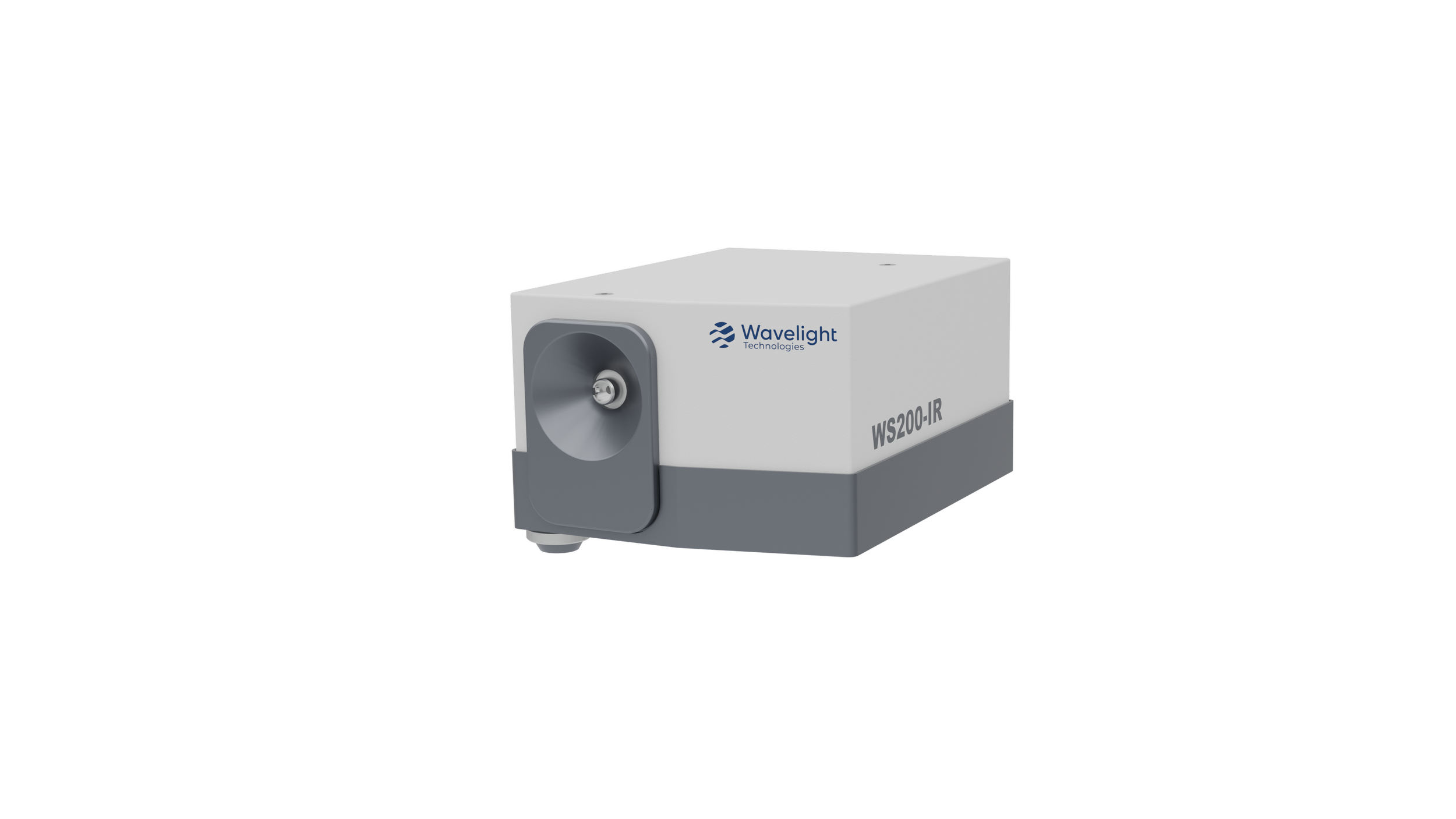
Supercontinuum lasers, often referred to as “white light lasers,” have emerged as a turn-key fiber-laser technology widely used across fields ranging from biomedical imaging to optical device characterization. Their popularity stems from a unique combination of broad spectral coverage, high output power, and diffraction-limited beam quality, making them a versatile and powerful light source for research and industrial applications.
Key Features
Extremely broad spectral range: 400 nm – 2400 nm
High optical output power: several watts
Diffraction-limited Gaussian beam: for precise focusing and imaging
Turn-key operation: fully integrated fiber-based systems for ease of use
How It Works
Most commercial supercontinuum sources are fully fiber-based, consisting of:
A mode-locked fiber oscillator serving as the master seed laser, typically producing picosecond pulses around 1064 nm with repetition rates in the tens of MHz.
A fiber amplifier to boost the pulse peak power.
A few meters of photonic crystal fiber (PCF) with engineered dispersion, where nonlinear interactions generate the broadband supercontinuum output.
When combined with a tunable spectral filter, the supercontinuum laser transforms into a widely tunable light source, enabling flexible and precise control over the output wavelength for a variety of scientific and industrial applications.
Applications
Supercontinuum lasers are highly versatile and are used in:
Biomedical imaging (e.g., optical coherence tomography, multiphoton microscopy)
Spectroscopy and optical characterization of materials and devices
Laser-based metrology and high-resolution imaging
Nonlinear optics and photonics research
With their unmatched spectral coverage, tunability, and high beam quality, supercontinuum sources provide a reliable and adaptable platform for both research and industrial applications requiring broadband, high-intensity light.
-
Axiom Optics provides complete Particle Image Velocimetry (PIV) systems developed in collaboration with OPTOLUTION and William Thielicke, the developer of PIVlab. These systems are specifically designed for seamless operation with PIVlab, a free, open-source software platform for quantitative PIV analysis. PIVlab is widely recognized as one of the most accessible and extensively cited PIV software tools, and is trusted by a global community of academic and industrial researchers.
The offered PIV systems are optimized for synchronized hardware–software integration, enabling precise flow-field measurements with minimal setup complexity. In addition to native compatibility with PIVlab, the systems support flexible integration with third-party components and alternative data acquisition workflows, allowing users to operate independently of PIVlab if required.
Axiom Optics supplies a comprehensive range of PIV hardware components compatible with PIVlab, including pulsed laser diode illumination sources, timing and synchronization units, high-speed and scientific cameras, and seeding particle generators. All components can be remotely controlled directly through the PIVlab interface, facilitating automated operation, reproducibility, and accurate temporal synchronization for advanced flow diagnostics.
-
Terahertz Time-Domain Spectroscopy (THz-TDS) is a cutting-edge technique for probing intermolecular interactions and characterizing the properties of solid materials. Operating in the 0.1–10 THz spectral range, THz-TDS utilizes low-energy, non-ionizing radiation, making it a safe and highly versatile tool for research and industrial applications.
Key Features
Simultaneous amplitude and phase measurement for complete material characterization
Non-ionizing radiation, safe for biological tissues
High transparency for many materials, enabling contact-free measurements
Suitable for metals, semiconductors, 2D materials, and superconductors
Applications
THz-TDS is widely used in fields such as:
Material characterization and process control
Contact-free conductivity measurements of advanced materials
Chemical identification of amino acids, peptides, pharmaceuticals, and explosives
Security and biomedical applications, leveraging its safe and non-destructive nature
With its combination of safety, precision, and versatility, THz-TDS has become an essential technique for fundamental science, advanced materials research, and high-stakes industrial and medical applications.
-
Key Features
Simultaneous amplitude and phase measurement for complete material characterization
Non-ionizing radiation, safe for biological tissues
High transparency for many materials, enabling contact-free measurements
Suitable for metals, semiconductors, 2D materials, and superconductors
Applications
THz-TDS is widely used in fields such as:
Material characterization and process control
Contact-free conductivity measurements of advanced materials
Chemical identification of amino acids, peptides, pharmaceuticals, and explosives
Security and biomedical applications, leveraging its safe and non-destructive nature
With its combination of safety, precision, and versatility, THz-TDS has become an essential technique for fundamental science, advanced materials research, and high-stakes industrial and medical applications.
-
Pump-probe spectroscopy is a powerful ultrafast technique that enables direct observation of dynamic processes in molecules, materials, and complex systems on femtosecond to picosecond timescales. By using two precisely timed light pulses—a pump pulse to excite the system and a delayed probe pulse to monitor its response—researchers can capture transient phenomena such as electronic and vibrational excitations, energy transfer, photochemical reactions, particle motion, plasma formation, and structural changes. By varying the delay between pulses, the temporal evolution of these processes can be mapped with exceptional precision. Advanced experimental methods, including transient absorption, four-wave mixing, and sum-frequency generation, allow the collection of time-resolved signals across spectral ranges from UV and X-ray to far-infrared. Tunable pump and probe pulses enable two-dimensional spectroscopy, producing temporally resolved energy maps that reveal both independent and coupled states of the system. This technique provides unmatched insight into ultrafast dynamics, making it indispensable for fundamental research in photochemistry, materials science, and molecular physics.
-
Thomson scattering is a key technique for plasma diagnostics in nuclear fusion devices, including tokamaks and stellarators. It allows precise measurement of electron temperature and electron density across multiple locations within the plasma.
How It Works
A pulsed laser is directed into the plasma.
Free electrons scatter the laser light, producing a spectral expansion due to the Doppler effect.
Photon detectors capture the scattered light, while high-speed digitizers record the resulting waveforms.
The spectral broadening provides information on the plasma temperature, and the scattered photon count determines plasma density.
Key Considerations for Data Acquisition
Thomson scattering experiments often involve hundreds of measurement channels, making scalable and modular instrumentation essential. Critical factors for digitizer selection include:
High dynamic range: Accurate measurement of pulse characteristics and determination of plasma density.
High analog bandwidth and sampling rate: Match detector performance and ensure high spatial resolution.
Compact and scalable form factor: High channel density reduces system size and the number of boards required.
Accurate and flexible triggering: Synchronization with the laser is crucial.
Backplane or integrated synchronization: Ensures precise multi-channel data capture with minimal external cabling.
Sufficient memory: Store complete scattered waveforms for each pulse.
High data throughput: Enable transfer of large amounts of data to a central processing unit between pulses.
Real-time processing capability: On-board processing can reduce data volume and improve efficiency.
Applications and Benefits
Fusion research: Monitor plasma behavior in real-time to optimize performance.
Temperature and density profiling: Provides detailed spatial maps of plasma parameters.
Scalable multi-channel systems: Modular instruments allow expansion as experimental requirements grow.
Customizable processing: Real-time calculations and data reduction can be implemented for specific experimental needs.